- 您现在的位置:买卖IC网 > Sheet目录3827 > PIC16F877A-I/P (Microchip Technology)IC MCU FLASH 8KX14 EE 40DIP
PIC16F87XA
DS39582B-page 46
2003 Microchip Technology Inc.
4.3
PORTC and the TRISC Register
PORTC is an 8-bit wide, bidirectional port. The corre-
sponding data direction register is TRISC. Setting a
TRISC bit (= 1) will make the corresponding PORTC
pin an input (i.e., put the corresponding output driver in
a High-Impedance mode). Clearing a TRISC bit (= 0)
will make the corresponding PORTC pin an output (i.e.,
put the contents of the output latch on the selected pin).
PORTC is multiplexed with several peripheral functions
(Table 4-5). PORTC pins have Schmitt Trigger input
buffers.
When the I2C module is enabled, the PORTC<4:3>
pins can be configured with normal I2C levels, or with
SMBus levels, by using the CKE bit (SSPSTAT<6>).
When enabling peripheral functions, care should be
taken in defining TRIS bits for each PORTC pin. Some
peripherals override the TRIS bit to make a pin an
output, while other peripherals override the TRIS bit to
make a pin an input. Since the TRIS bit override is in
effect while the peripheral is enabled, read-modify-
write instructions (BSF, BCF, XORWF) with TRISC as the
destination, should be avoided. The user should refer
to the corresponding peripheral section for the correct
TRIS bit settings.
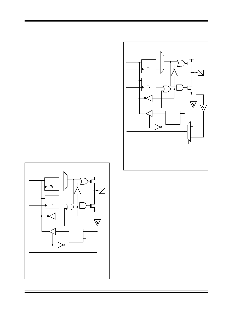
FIGURE 4-6:
PORTC BLOCK DIAGRAM
(PERIPHERAL OUTPUT
OVERRIDE) RC<2:0>,
RC<7:5>
FIGURE 4-7:
PORTC BLOCK DIAGRAM
(PERIPHERAL OUTPUT
OVERRIDE) RC<4:3>
Port/Peripheral Select(2)
Data Bus
WR Port
WR TRIS
Data Latch
TRIS Latch
Schmitt
Trigger
Q
D
Q
CK
QD
EN
Peripheral Data Out
0
1
Q
D
Q
CK
P
N
VDD
VSS
RD Port
Peripheral
OE(3)
Peripheral Input
I/O
pin(1)
Note 1: I/O pins have diode protection to VDD and VSS.
2: Port/Peripheral Select signal selects between port
data and peripheral output.
3: Peripheral OE (Output Enable) is only activated if
Peripheral Select is active.
RD TRIS
Port/Peripheral Select(2)
Data Bus
WR Port
WR TRIS
Data Latch
TRIS Latch
Schmitt
Trigger
Q
D
Q
CK
QD
EN
Peripheral Data Out
0
1
Q
D
Q
CK
P
N
VDD
VSS
RD Port
Peripheral
OE(3)
SSP Input
I/O
pin(1)
Note 1: I/O pins have diode protection to VDD and VSS.
2: Port/Peripheral Select signal selects between port data
and peripheral output.
3: Peripheral OE (Output Enable) is only activated if
Peripheral Select is active.
0
1
CKE
SSPSTAT<6>
Schmitt
Trigger
with
SMBus
Levels
RD TRIS
发布紧急采购,3分钟左右您将得到回复。
相关PDF资料
MP2-HS240-51
CONN SHROUD 2-FB 240POS 5ROW
DSPIC33FJ64MC506-I/PT
IC DSPIC MCU/DSP 64K 64TQFP
DSPIC33FJ128MC802-I/SO
IC DSPIC MCU/DSP 128K 28SOIC
PIC18LF4331-I/P
IC PIC MCU FLASH 4KX16 40DIP
DSPIC33FJ128GP306-I/PT
IC DSPIC MCU/DSP 128K 64TQFP
PIC24HJ128GP306-I/PT
IC PIC MCU FLASH 128KB 64TQFP
PIC16F873-20/SO
IC MCU FLASH 4KX14 EE 28SOIC
PIC18F4431-I/P
IC PIC MCU FLASH 8KX16 40DIP
相关代理商/技术参数
PIC16F877A-I/P
制造商:Microchip Technology Inc 功能描述:IC 8BIT FLASH MCU 16F877 DIP40
PIC16F877A-I/PG
功能描述:8位微控制器 -MCU 14KB 368 RAM 33 I/O RoHS:否 制造商:Silicon Labs 核心:8051 处理器系列:C8051F39x 数据总线宽度:8 bit 最大时钟频率:50 MHz 程序存储器大小:16 KB 数据 RAM 大小:1 KB 片上 ADC:Yes 工作电源电压:1.8 V to 3.6 V 工作温度范围:- 40 C to + 105 C 封装 / 箱体:QFN-20 安装风格:SMD/SMT
PIC16F877A-I/PT
功能描述:8位微控制器 -MCU 14KB 368 RAM 33 I/O RoHS:否 制造商:Silicon Labs 核心:8051 处理器系列:C8051F39x 数据总线宽度:8 bit 最大时钟频率:50 MHz 程序存储器大小:16 KB 数据 RAM 大小:1 KB 片上 ADC:Yes 工作电源电压:1.8 V to 3.6 V 工作温度范围:- 40 C to + 105 C 封装 / 箱体:QFN-20 安装风格:SMD/SMT
PIC16F877A-I/PT
制造商:Microchip Technology Inc 功能描述:8BIT FLASH MCU SMD 16F877 TQFP44
PIC16F877A-I/PTG
功能描述:8位微控制器 -MCU 14KB 368 RAM 33 I/O RoHS:否 制造商:Silicon Labs 核心:8051 处理器系列:C8051F39x 数据总线宽度:8 bit 最大时钟频率:50 MHz 程序存储器大小:16 KB 数据 RAM 大小:1 KB 片上 ADC:Yes 工作电源电压:1.8 V to 3.6 V 工作温度范围:- 40 C to + 105 C 封装 / 箱体:QFN-20 安装风格:SMD/SMT
PIC16F877AIL
制造商:Microchip Technology Inc 功能描述:
PIC16F877AIP
制造商:Microchip Technology Inc 功能描述:
PIC16F877AIPT
制造商:Microchip Technology Inc 功能描述: